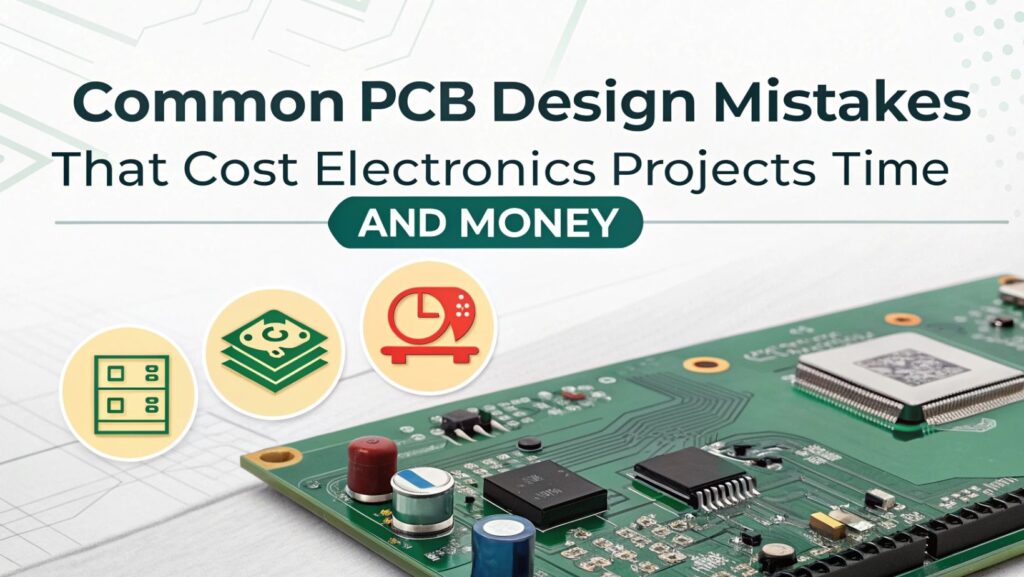
Imagine this: you have spent weeks refining your circuit design, carefully choosing components, and at last sent your PCB off for manufacture. Then, the harsh reality sets in—your boards display issues that were easily preventable. Not unfamiliar? You are not alone. Although most costly PCB design errors can be completely avoided if you know what to look for, even seasoned engineers can still fall into these traps.
Let’s examine the most often occurring mistakes that might ruin your electronics projects and, more importantly, how to avoid them.
The Nightmare of the Ground Plane
One of the most often occurring errors I find is poor ground plane design. Many designers consider ground connections as an afterthought, either depending on a few via connections or producing thin traces. Ground loops, electromagnetic interference (EMI), and erratic circuit behavior can all follow from this method.
Your circuit’s foundation is a correct ground plane. It lowers noise, provides a low-impediment return path for current, and aids in heat dissipation. Skimp on the ground plane design, and you are effectively building your electronic house on unstable ground. The outcome is circuits on your breadboard that fail spectacularly on the PCB.
In multi-layer designs, commit an entire layer to the ground, or guarantee generous ground plane coverage in two-layer boards to prevent this expensive mistake. Consider your ground plane as prime real estate; let it not become scattered islands.
Traversal Width Problems
Incorrect trace width calculations constitute still another wallet-draining error. Many projects I have seen involve designers either making traces unnecessarily thick, wasting valuable board space and increasing costs, or making traces too thin, causing voltage drops and heating problems.
The secret is to know how copper thickness, trace width, and current-carrying capacity relate to one another. A trace too small for its present load will heat up and possibly damage components or cause dependability problems not seen until your product is in use. Conversely, traces that are too wide can complicate routing and unnecessarily increase the size of the board.
Use trace width calculators and always consider temperature rise. Recall that one amp of trace requires different dimensions than one carrying 100 milliamps. In doubt, err on the side of caution, but do not go too far.
By Violations
Although vias appear to be simple connections between layers, they can frequently lead to significant problems. The most common errors include failing to consider via-in-pad needs for fine-pitch components, using an insufficient number of vias for high-current paths, or placing vias too close to component pads.
Every via has inductance and resistance, which might not seem like much but in high-frequency or high-current applications can add up rapidly. Often for power connections, several vias in parallel are required. Via location can significantly compromise signal integrity in sensitive analog circuits.
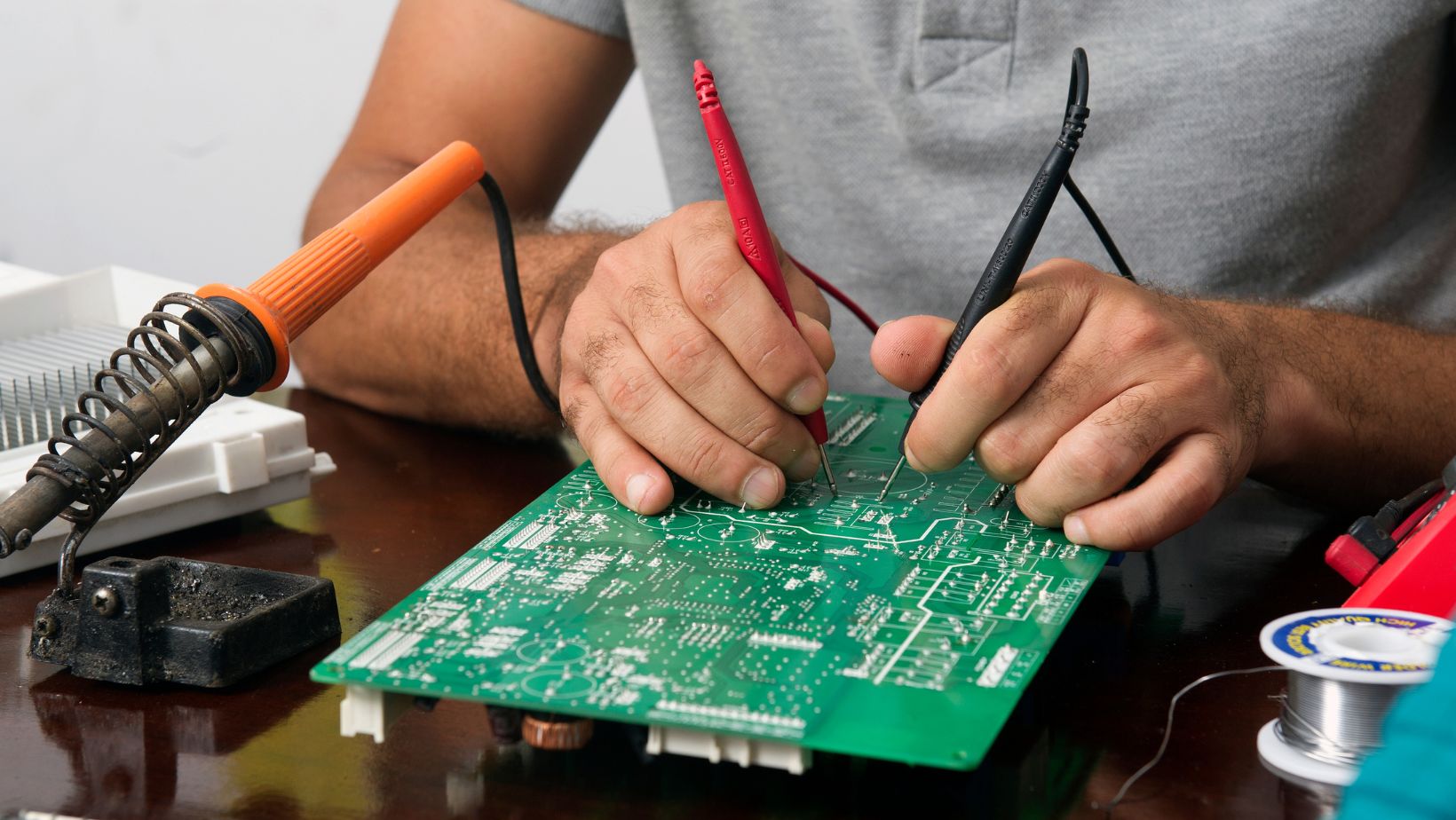
Expert PCB makers, such as WellPCB, frequently find designs that could have been improved with better planning. Spending time during the design process to understand the specifications and placement guidelines helps avoid costly responses later.
Component Arrangement Chaos
Bad component placement is like setting furniture without thinking about how people will move about the room. I have seen boards where high-speed digital circuits sit directly next to sensitive analog sections, generating almost impossible-to-fix noise coupling problems without a total overhaul.
Placed without thermal consideration, heat-generating components can produce hot spots influencing surrounding components. Similarly, placing components too close together can make assembly challenging or even impossible, leading to manufacturing yields that could make your accountant cringe.
The answer calls for considering signal flow, thermal control, and manufacturing restrictions during placement. Always consider how the board will be built and tested; group related circuits together, and keep noisy digital sections away from quiet analog ones.
Design of Power Supply Disaster
Unstable power sources kill a project more quickly than anything else. Typical errors include inadequate decoupling capacitors, poor power distribution planning, and neglect of voltage drop calculations generally.
 Correct operation of every integrated circuit depends on stable, clean power. This means putting decoupling capacitors near power pins, using suitable capacitor values for various frequency ranges, and making sure your power distribution network can manage current demands without too great a voltage drop.
Power supply noise can show up as digital circuits that periodically fail, analog circuits with poor performance, or communication interfaces that work sometimes but not others. Preventing issues is much less expensive than debugging these sporadic problems later.
Oversights of Signal Integrity
Signal integrity becomes critical as clock speeds rise and signal edges get sharp. These days, length matching, controlled impedance, and appropriate termination are not only high-speed design issues; they also impact most contemporary digital circuits.
Problems like signal reflections, crosstalk, and timing errors in differential pairs can happen if trace lengths are not the same, if the characteristic impedance is wrong, or if terminating resistors are missing. These problems might not stop your circuit from working totally, but they can cause sporadic failures that are costly to debug and repair.
Most signal integrity issues can be avoided by knowing transmission line theory and applying simulation tools throughout design. Treating traces as transmission lines becomes critical when signals pass faster than your coffee break.
Thermal Control Mistakes
Despite the fact that heat poses a significant threat to electronics, we often overlook thermal issues until they become problematic. Components running too hot not only fail; they also degrade over time, compromising long-term dependability and maybe posing safety concerns.
Effective thermal control calls for more than just a heat sink. Within your PCB design, it calls for knowledge of heat sources, heat paths, and heat sinks. Through arrays, copper pours can distribute heat between layers; component placement can help to avoid hot spots.
Thermal simulation conducted during the design process helps identify possible issues before they become costly failures. Recall, a component running cool performs better and lasts longer.
Proceeding With Confidence
While learning from others’ experiences is far more affordable, PCB design errors are costly teachers. The secret is creating a methodical approach starting from the beginning of your design process that takes mechanical, electrical, thermal, and manufacturing constraints into account.
Remember that prevention is always cheaper than correction. While spending more time on design review, simulation, and verification may seem to be slowing down your project, in fact it is accelerating your road to a successful product.